Lithography Optics Inspection
Lens inspection using 193 nm and 248 nm
- Inspection of lithography optics with coherent cw laser light
- Using wavelengths of 193 or 248 nm (Excimer laser wavelengths)
- For highest spatial resolution state-of-the-art diode lasers are preferable
- TOPTICA's frequency-stabilized and frequency-converted lasers are ideal tools
Photolithography is a microfabrication technique that is commonly used to pattern parts of a thin film or the bulk of a substrate. It is also often termed as optical lithography or UV lithography, if ultraviolett wavelengths are used.
The techninque uses light to transfer a geometric pattern from a photomask onto a light-sensitive chemical ("photoresist" or "resist") on the substrate. This first irradiation step is followed by a series of chemical treatments that either engrave the exposed pattern into the material underneath the photo resist, or it enables deposition of a new material in the desired pattern on top of it.
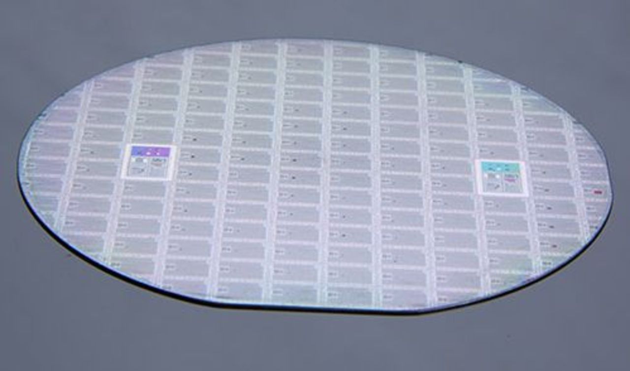
For example, to produce complex integrated circuits, a state-of-the-art CMOS wafer goes up to 50 times through the described photolithographic cycle. In photolithography systems usually deep ultraviolet excimer lasers like the krypton fluoride laser at a wavelength of 248 nm or the argon fluoride laser at 193 nm wavelength are used.
The optical lens system of photolithography setups is usually very complex and consists of an extensive combination of various lenses in order to achieve highest spatial resolution. These lenses are inspected during the manufacturing process with coherent cw laser light of the same wavelength as the excimer lasers, i.e. 193 or 248 nm. Since excimer lasers are very non-coherent lasers regarding their spatial resolution, other lasers are used for this inspection, e.g. frequency-stabilized and frequency-converted diode lasers.