Semiconductor Inspection & Metrology
Semiconductors are the backbone of the modern world. From smartphones to datacenters, medical devices to autonomous vehicles, semiconductors form the foundation of nearly every innovation in the digital age. Particularly, the rise of Generative AI has fueled an insatiable demand for computation and memory. Training Large Language Models (LLMs) depends on large clusters of GPU and High-Bandwidth Memory (HBM) stacks of multiple layers of DRAM, which are produced on leading-edge semiconductor nodes.
The industry is addressing the demand for continued scaling by embracing ≤3nm design nodes, novel 3D-transistor designs and stacked chip architectures, where transistors are vertically layered to increase processing power while reducing footprint and energy consumption. In the back-end, heterogeneous integration, and advanced, wafer-scale packaging technologies are employed to optimize performance, latency, power efficiency.
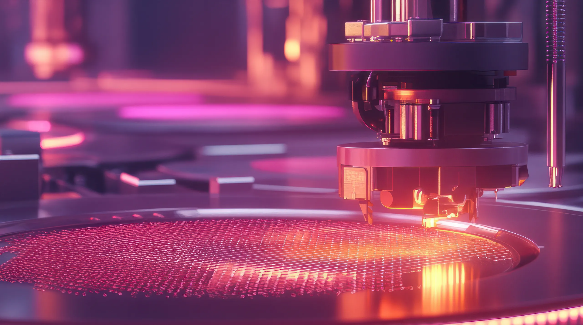
With shrinking feature sizes, more & thinner layers as well as increasing chip and package areas, the cost of damage of a wafer in the fab keeps rising continuously. At the same time, every sub-nanometer deviation during the manufacturing process (e.g., in line width, film thickness, overlay) can cause device failure or yield loss. As a result, Metrology and Inspection tools become even more vital. From patterning to packaging, every step must be measured, verified, and optimized. By characterizing materials and calibrating process equipment in real-time, Metrology and Inspection techniques are able to identify opportunities for yield improvement, ultimately lowering production costs. This comprehensive approach enhances the yield and cost-scaling of next-generation semiconductor devices, essentially keeping Moore's Law alive.
Laser-based metrology and inspection have become indispensable tools for achieving these goals — enabling manufacturers to visualize, quantify, and understand structures that are far smaller than the wavelength of visible light. Together with our customers, TOPTICA enables Semicon manufacturers to increase yield and throughput by optimizing key parameters like overlay accuracy, defect detection rates, wafer coverage and higher resolution across a variety of modalities including optical, e-Beam and THz.

In Optical Scatterometry (Optical Critical Dimensions), coherent laser light probes periodic nanostructures to determine profile, dimensions, and material properties of periodic structures on a wafer. The reflected diffraction pattern is analyzed to extract critical dimensions with sub-nanometer precision. Tunable and narrow-linewidth diode lasers provide the spectral stability and wavelength flexibility essential for accurate modeling of advanced nodes.

Ellipsometry determines film thickness, refractive index, and composition by analyzing polarization changes of reflected laser light. With narrow spectral linewidths and stable polarization, lasers deliver unmatched repeatability. Imaging ellipsometers, illuminated by polarized laser sources, allow rapid mapping of film uniformity across full wafers.

Terahertz time-domain spectroscopy (THz-TDS) allow for contact-free, fast, and spatially resolved measurement of charge carrier density and mobility - key parameters e.g. for power electronics and high-end RF chips based on compound semiconductors like silicon carbide (SiC) or gallium nitride (GaN). The technique works under ambient conditions, without any electrodes or surface preparation and eliminates the risk of wafer damage of contamination.

Laser interferometry provides non-contact, high-accuracy measurements of surface properties, film thickness, and topography. The coherence and phase stability of laser sources enable sub-nanometer height resolution. By using a controlled phase shift in an interferometer, one creates a series of intensity images, which are then processed to precisely determine the phase and amplitude of light waves. The technique is also being used to obtain a high-resolution, 3D surface map of lenses or other optical components.

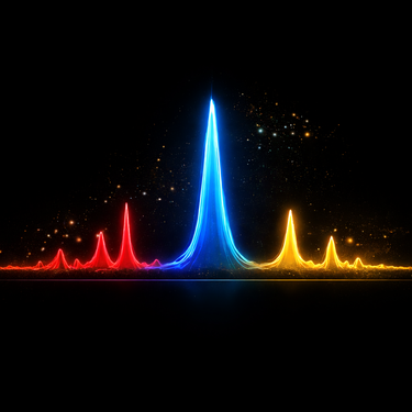
Raman spectroscopy is a non-destructive analytical technique based on the inelastic scattering of monochromatic light. When a laser photon interacts with a molecule or crystal lattice, a small fraction of photons is scattered at shifted frequencies that are characteristic of the vibrational modes of the material. These frequency shifts—the Raman spectrum—serve as a molecular fingerprint for chemical identification, structural characterization, and quantitative analysis.
From process diagnostics to materials research, laser-based metrology is the foundation of precision in the semiconductor industry.
TOPTICA’s narrow linewidth diode and ultrafast laser systems provide the stability, wide wavelength coverage and spectral purity required to meet the most demanding inspection and metrology challenges of today’s and tomorrow’s semiconductor technologies.